CPU Overview
Cores - a unit that can independently execute a thread. Usually multiple cores are present on a chip e.g. Dual Core or Quad Core chips.
Chip - is a single or multi core physically integrated circuit.
Socket - physical connector on a motherboard that accepts a single chip. Motherboards can have multiple sockets, each socket has one chip fitted in it, this chip can have one or more cores.
Note - Usually, the terms used are Socket and Cores. Frequently the terms Sockets, Chips and CPUs are used interchangeably.
Hyper-Threading - Single core used for concurrent execution of two or more thread, using extra hardware but not replicating the entire core.
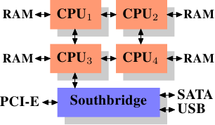
Front Side Bus (FSB) - Multiple CPUs are connected via the FSB to the Northbridge.
Northbridge - contains the memory controller and other hardware. The memory controller determines the type of RAM that can be connected to the CPUs. Northbridge mainly connects the CPUs to the RAM.
Southbridge - is the I/O bridge, handles communication with devices through various buses i.e. PCI, PCI Express, SATA and USB buses.
Northbridge connects to the Southbridge. All communication between the CPU and a device connected to Southbridge is routed via the Northbridge.
Communication between CPUs travels over the same FSB which is also used to communicate with the Northbridge.
Communication with RAM passes through the Northbridge.

Direct Memory Access (DMA) - allows devices connected to the Southbridge to directly read and write to the RAM via the Northbridge without adding workload on the CPU. However the Northbridge becomes a bottleneck as it is used for both DMA access to RAM and CPU access to RAM.
The bus from Northbridge to RAM can also become a bottleneck as access to all RAM chips is done via the same bus. DDR2 RAM doubles this bandwidth by having two separate buses.
With multiple cores and multiple sockets the requirement for RAM access increases and the Northbridge to RAM bus becomes a bottleneck. There are designs that work around this.
Northbridge with External Memory Controllers (MC) - is a technique where there are multiple MCs connected to the northbridge and each MC is connected to a RAM. The CPUs are connected to the northbridge via separate FSBs instead of a common FSB. This design increases the bandwidth for memory transfer to/from the CPU.
Non Uniform Memory Access (NUMA) - CPUs with Integrated Memory Controllers - where each cpu has its own memory controller and a RAM connected to it. The CPUs in turn are connected to each other, so that all the memory is available to all the CPUs. AMD Opteron and Intel Nehalem support this design.
In NUMA design, the local memory i.e. RAM connected to the CPU is accessible the fastest, however RAM connected to another CPU is accessible at a lower speed as the access involves routing through an intermediate CPU.
RAM Types
SRAM - Static random access memory. Faster than DRAM but more expensive. It consists of 6 transistors and requires constant power to maintain state. SRAM is used for CPU caches.
DRAM - Dynamic random access memory. It consists of 1 transistor and 1 capacitor. The simple design of DRAM cell implies that it requires lesser space compared to SRAM. The capacitor discharges after every read operation and thus needs a recharge after every read. Additionally, the capacitor leaks i.e. the DRAM cell needs to be recharged constantly (every 64ms). During a refresh cycle, no access to memory is possible. The recharge after read implies that the DRAM cell isn't available for a subsequent read.
DRAM Access - When a program selects a memory location using a virtual address it is converted by the Memory Management Unit into a physical address and given to the Memory Controller which selects the RAM chip corresponding to that address. This selection of RAM chip and the address of cells within the chip is done using Row and Column selection i.e. the DRAM cells are not arranged as an array but instead in row-column form so that a small number of lines (on the bus i.e. bus width) is required.
Note - every cell requires a recharge every 64ms which implies that for a DRAM with thousands of cells a recharge cycle is being initiated for a cell at a much smaller time gap. Since cells are organized in rows and column, the recharge cycle is done for all cells in one row. A DRAM with 8192 rows requires that a recharge cycle be started every 7.8125us (64 / 8192).
Other RAM Types -
- Asynchronous DRAM
- RDRAM - Rambus DRAM
- SDRAM - Synchronous DRAM
- DDR DRAM - Double Data Rate DRAM
- SDR SDRAM - Single Data Rate SDRAM, also known as SDR
- DDR SDRAM - Double Data Rate SDRAM, also known as DDR1
- DDR2 SDRAM
- DDR3 SDRAM
- FB-DRAM - Fully Buffered DRAM
SDRAM works relative to a time source. The memory controller provides a clock whose frequency determines the speed of the FSB. These frequencies are usually 800MHz, 1333MHz, etc. The data transfer from SDRAM is done two or four times per cycle i.e. 2*1333MHz or 4*1333MHz. SDRAM manufacturers advertise this effective bus speed i.e. 2,666MHz SDRAM.
CPU Cache
CPU clock speeds have improved significantly. Hard drive (HDD/SSD) and RAM read/write/seek speeds haven't increased at the same rate and neither has the bus speed i.e. FSB connecting CPU to RAM. Faster RAM i.e. SRAM is available with comparable bus speeds to connect to the CPU - however the high cost makes them uneconomical.
CPU designers have put in caches i.e. small amounts of SRAM to contain copies of sub-sets of main memory (DRAM). Cache allows much faster access compared to RAM.
Note - Cache's are managed by the processor and not by the OS.
Spatial Locality - Over short periods of time same code or data gets accessed. Code - programs usually contain loops in code so the same code gets executed repeatedly. Data - access to data in a small region.
Temporal Locality - Over a period of time same memory location is accessed repeatedly i.e. a function called often leads to a jump in code to the same memory location where the function is loaded or data (global, singleton) is reused.
The time to access cache or main memory is measured in CPU cycles. The ratio of access time for cache:main memory could be 1:15 i.e. accessing data in cache would require 1 cycle compared to 15 cycles if it were present in main memory. In this example cache's offer up to 93% improvement. Since SRAM is used for caches their size is limited compared to main memory.
CPUs are connected to Caches which are connected to the Main Memory i.e. CPUs and Main Memory are not connected directly. All memory read, write is done via the cache.
Caches for code and data are kept separate as the memory regions of code and data are independent of each other. Thus L1d and L1i caches represent data and instruction/code respectively. Further, instruction decoding is a slow process thus caching decoded instructions speeds up execution.
Usually machines have three levels of caches L1, L2 and L3 followed by RAM. The closer we move towards the CPU the smaller the memory size and faster access time. Registers are closes to the core i.e. fastest access time between core and L1 cache.
Multi-processors machines have multiple CPUs, each CPU has multiple cores, each core has its own set of L1 cache. Cores within a processor share L2 and L3 cache. Multiple threads running on a core share the L1 cache. Each thread has its own set of registers. This is a general CPU design, recent generation of CPUs may change as designers search for better performance.
Todo - read more about memory regions which cannot be cached and about instructions (programming) to bypass the cache.
Programs access memory using virtual addresses. Virtual address can be used to access the cache or converted to physical address prior to cache access - this depends on the cache implementation. Most cache implementation use virtual addresses to tag the cache lines in L1 cache and physical addresses for L2 and L3 caches. The L1 cache access time is lowest, thus the translation from virtual to physical address would take longer then accessing the cache directly with virtual address. The L2 and L3 cache access time is higher and translation from virtual to physical address is comparatively small.
Transition Look-aside Buffer (TLB) is a cache of virtual to physical address translations.
Since caches contain a subset of main memory the cache entries are tagged using the address of the same data word in main memory. Read/write requests are first checked in cache for a matching tag.
Note - Word size is equal to the FSB bus width, cpu register size i.e. 64-bit processor has a word size of 64 bits, its FSB is 64 bits wide and the registers are 64 bits.
Cache Lines - Each memory location in the cache and main memory has a size of one word. When content is loaded from main memory to cache it is done in multiples of word size to account for spatial locality. As RAM cells are arranged in rows and columns, a row contains multiple words and one or more rows are loaded into the cache as part of a load operation. These are known as cache lines.
Dirty Cache Line - When a program attempts to reads a data element, it leads to a cache line load which could be longer than the size of the data element. After the cache line is loaded, the data element can be read and if the program attempts to write to it, the cache line is updated and flagged 'dirty'. This dirty cache line contains and updated and modified contents which have not yet been written back to main memory. Once written back, the dirty flag is cleared.
Cache Eviction - To load data into the cache, it must have free space. If there is no free space, a cache line from L1d is pushed to L2. If L2 does not have free space a cache line is pushed from L2 to L3. Similarly L3 cache lines are pushed out to main memory. Each eviction is progressively expensive. Most caches uses the Least Recently Used (LRU) element first.
Note - L1d caches contain data, which is modifiable. L1i contains code which cannot be modified.
Exclusive vs Inclusive Caches - Intel implements inclusive caches, where on a load instruction data is copied from main memory to each cache line i.e. L3, L2 and L1d. When evicting a cache line not marked dirty, the process is faster as the line from L1d can be overwritten without having to copy it to L2 or L3. AMD implements exclusive caches, where on a load instruction data is copied from main memory to L1d without touching L2 or L3. This leads to a faster load operation. However on eviction the cache lines need to progressively evicted.
Todo - read more about inclusive and exclusive cache design.
Cache Coherency - Symmetric Multi-Processor systems have multiple CPUs and each CPU has its own cache. These caches can't work independently i.e. all processors should see the same memory content at all times. To maintain this uniform view, cache coherency protocols are used. The intent is to implement these two rules -
- a dirty cache line is not present in more than one processor's cache
- clean cache lines can reside in multiple caches
Coherency implementations -
- Write-Through - is the simple (but not fast) approach, any cache line which is written to is immediately written back to main memory. This ensures consistent between main memory and cache. Cache eviction can simply remove the line from the cache. A program which modifies the same local variable over and over would create a lot of traffic on the FSB even though this data may not be accessed anywhere else.
- Write-Back - is more sophisticated, the processor does not write back cache lines, instead it marks them dirty. Cache eviction will prompt the processor to write back a dirty line before removing it from the cache. Processors can use free capacity on the FSB i.e. when there is no traffic to write back dirty cache lines and on eviction simply drop them from the cache. When more than one processor are present, and one of them accesses a cache line marked dirty in the other processors cache, the line must be synchronized.
- Write-Combining - is an optimization used in devices such as graphics cards, where multiple writes are combined before the cache line is written to the device. Usually neighboring pixels on a screen are on the same cache line and need to written to sequentially, once the writes are complete the cache line is written to the RAM.
- Uncacheable Memory - are memory location that are not backed by RAM. These are special addresses hardcoded to have some functionality outside the CPU, for e.g. memory mapped address ranges which translate to accesses to cards and devices attached to a bus.
Cost of accessing in count of cycles -
- Register ~ 1
- L1d ~ 3
- L2 ~ 14
- Main Memory ~ 240
Instruction Pipeline - processors load and decode subsequent instructions, based on a predicted code branch, to keep them execution ready. This process of preloading allows reducing (hiding) the time to load instructions and data across caches and main memory. The instructions that can preloaded is limited for e.g. write instructions whose value to be written depend on the output of previous instructions can't be decoded and similarly branches that cannot be predicted or are incorrectly predicted do not offer any benefit. The intend of preloading is to hide/reduce the amount of time spent in loading instruction and data sequentially.
Todo - read more on prefetching, pipleine, decoding.
Working Set & Cache Performance
Drepper lists an interesting experiment with different working sets. A simple struct is defined which contains a pointer of the same type and an array of type long int -
struct data {
struct data * next;
long int pad[N];
}
N=0 - creating a list of smaller data elements and sequentially traversing over the list shows performance which is directly proportional to the cost of accessing various cache levels.
N=7 vs N=31 - creating a list of mid size data elements vs large data elements and sequentially traversing over the lists shows gap in performance varies as the working set grows. The hardware prefetcher is unable to optimize as the data crosses page boundaries. Additionally the TLB cache misses add to the degradation in performance.
Todo - read more to understand in detail how the Memory Controller, Memory Management Unit and TLB work together.
When the same lists are traversed randomly the TLB misses penalty adds significantly and the performance degrades. The degradation worsens as working set size grows.
Note - It is possible (and should be mandatory) for developers to look at widely used data structures in their code, note the size of each element, the collection type used i.e. list, queue, tree, the access mode i.e. random vs sequential and measure the performance of their code keeping into account the cache sizes. A system intended for high throughput should be optimized keeping this in mind. Proper hardware purchase decisions can be made with these tests.
MESI Cache Coherency Protocol
Coherency becomes complicated when multiple processors with their own caches need to access cache lines which may have been modified by another processor. A similar problem exists for multiple cores in a processor, with their own L1d cache and a shared L2 or L3 cache.
The write-back policy can be efficiently implemented using these four states -
- Modified - cache line is modified by local processors and it is the only copy in any of the caches.
- Exclusive - cache line is not modified and not loaded in any other processors cache.
- Shared - cache line is not modified and may be in another processors cache.
- Invalid - cache line is unused.
Initially all cache lines across all processors are marked invalid. If data is loaded to be written to the cache state is set to modified, if data is loaded for reading its state is set to exclusive if it hasn't been loaded by any other processor and if it has been loaded by another processor its state is set to shared.
If a processor loads and writes to a cache line it is set to Modified and is not written back to main memory. The processor can continue to modify or read the cache line. If a second processor attempts to read the cache line, the first processor sends the contents of its cache to the second processor and sets its state to Shared. The data sent to the second processor is also received by the memory controller which will store the contents in memory. This store in memory allows the cache line to be set to Shared state.
If the second processor requested to write to the cache line it sends a Request for Ownership (RFO), the first processors sends the contents of its cache and marks its cache as Invalid.
If the second processors initially requested to read the cache line (both processors set their cache line state to Shared) and then decides to write to the cache line then it sends a RFO and all other processors cache are marked Invalid, the processor than updates its cache line and marks it Modified.
Todo - read about multiple processors sending out RFO and arbitration mechanisms.
Note - The Exclusive state is similar to Shared state with a difference that a local write operation does not have to be announced on the bus. Thus a processor will attempt to keep as many cache lines as possible in the Exclusive state.
RFO messages are sent when -
- a thread is migrated from one processor to another and all cache lines need to be moved over to the new processor.
- a cache line is needed in two different processors.
Multi-thread and multi-process programs synchronize using memory which requires RFO messages.
MESI state transitions happen after all processors have responded to a message, thus the longest possible time to reply determines the speed of the protocol. Collisions are possible. NUMA systems exhibit high latency.
With multiple processors, the FSB is a shared resource and becomes a source for contention. The AMD Opteron design has separate RAM for each processor to reduce this contention but does not eliminate it, as multi-process programs will require synchronization of memory.
Note - thread synchronization makes use of this memory coherency protocol. the more locks are acquired/released the more strain is put on the system.
On a multi-processor system, when multiple threads access a collection of data elements, cache coherency (synchronization) and tlb misses add up to degrade performance.
Hyper-Threads (HT)
Also known as Symmetric Multi-Threading (SMT) allow a core to run multiple threads by sharing the L1 and other caches, but the register sets are not shared. Intel HT model supports two threads per core i.e. there are two sets of registers for the threads. When one thread is delayed (for memory access) the CPU can schedule another thread, thus time multiplexing them.
When the two threads scheduled as HT threads run two different sets of code and utilize two different sets of data, the cache size is effectively halved and the prefetch optimizations for one thread are of no use to the other thread. In this case the HT performance degrades as cache misses will be high.
HT is successful in limited situations, where the threads share the same instruction set and there is overlap in their data set. Further the cache hit rate of an individual thread should be low enough for the CPU to schedule the second thread and gain by running it during the delay time.
Instruction Cache
Both data and instructions are cached separately in the level 1 cache (L1d and L1i). The instruction cache has less complex issues associated with it.
The size of code is limited to the complexity of the problem, the instructions are generated by a compiler which understands good code generation versus data handling designed by programmers, program flow is more predictable compared to data access and code exhibits good spatial and temporal locality.
Instructions are executed in stages i.e. the CPU pipeline loads, decodes, prepares and executes an instruction over multiple stages. If the pipeline stalls because the next instruction cannot be correctly predicted or if it takes too long to load the next instruction the time to recover and refill the pipeline can be a while.
Todo - read more about Intel Netburst architecture.
Trace Cache - usually L1i cache contains instructions which have been decoded. This allows the processor to skip initial steps of the pipeline in case of a cache hit.
L2 caches are unified, contain both data and instructions. Instructions are in L2 cache are not decoded i.e. they are in raw byte format.
Todo - read about writing code with explicit prefetching.
L1i cache implementation does not use the MESI protocol, instead it uses a simplified SI protocol. This is because the code pages are expected to by read only.
Self Modifying Code (SMC) - is used in security exploits and performance optimization scenarios. SMC code complicates the L1i cache and instruction pipeline optimizations, when the processor detects code that has been modified it has to delete the pipeline and cache and start fresh.
Todo - read more on how to compile SMC code, tweaks for link time.
Critical Word Load & Early Restart
Transfer of data from main memory to the cache is done in blocks which are smaller than the cache line. Usually blocks are 64-bits and cache line size is 64 or 128 bytes. Thus a transfer involves 8 or 16 transfers per cache line.
When there's a cache miss in L1d or L1i, the data transfer is initiated from main memory and is expected to complete in 8/16 transfers where each transfer is 4 CPU cycles. If the CPU is interested in the first word on the cache line it can read this before the entire cache line transfer is complete. If the CPU is interested in the last word, it has to wait for the full transfer to complete before it can read the word.
Memory controllers have been optimized to request the words of the cache line in a different order. The word for which the processor is waiting is the critical word. This technique of requesting the critical word first is known as Critical Word First & Early Restart.
This isn't always feasible, for e.g. when prefetching data the processor does not know the location of the critical word.
Cache Placement
With hyper-threading the core allows both threads to have their own set of registers but they share the L1d and L1i cache.
With multiple cores, the past design used by Intel had dual core processor where each core had its own L1 caches and a common L2 cache. With the quad core processor, each core had its own L1 caches, a pair or cores shared L2 cache i.e. there were two sets of L2 caches for the two pair of cores. AMD processors had separate L2 cache for each core and unified L3 cache.
Todo - read on cache designs for more recent Intel and AMD processors. Intel has moved to three levels of cache in its latest design.
Note - there are ways to pin processes to cores, allowing programmers to distribute working sets across caches based on the capacity offered by the cpu.
FSB Speed
High speed FSBs are available which provide major improvements over slower FSBs. An important point to note is that though the FSB speed may be high the motherboard or northbridge might not support that speed. Large main memory with high speed FSBs offer significant benefits compared.
Cores - a unit that can independently execute a thread. Usually multiple cores are present on a chip e.g. Dual Core or Quad Core chips.
Chip - is a single or multi core physically integrated circuit.
Socket - physical connector on a motherboard that accepts a single chip. Motherboards can have multiple sockets, each socket has one chip fitted in it, this chip can have one or more cores.
Note - Usually, the terms used are Socket and Cores. Frequently the terms Sockets, Chips and CPUs are used interchangeably.
Hyper-Threading - Single core used for concurrent execution of two or more thread, using extra hardware but not replicating the entire core.
Front Side Bus (FSB) - Multiple CPUs are connected via the FSB to the Northbridge.
Northbridge - contains the memory controller and other hardware. The memory controller determines the type of RAM that can be connected to the CPUs. Northbridge mainly connects the CPUs to the RAM.
Southbridge - is the I/O bridge, handles communication with devices through various buses i.e. PCI, PCI Express, SATA and USB buses.
Northbridge connects to the Southbridge. All communication between the CPU and a device connected to Southbridge is routed via the Northbridge.
Communication between CPUs travels over the same FSB which is also used to communicate with the Northbridge.
Communication with RAM passes through the Northbridge.
source - wikipedia
Direct Memory Access (DMA) - allows devices connected to the Southbridge to directly read and write to the RAM via the Northbridge without adding workload on the CPU. However the Northbridge becomes a bottleneck as it is used for both DMA access to RAM and CPU access to RAM.
The bus from Northbridge to RAM can also become a bottleneck as access to all RAM chips is done via the same bus. DDR2 RAM doubles this bandwidth by having two separate buses.
With multiple cores and multiple sockets the requirement for RAM access increases and the Northbridge to RAM bus becomes a bottleneck. There are designs that work around this.
Northbridge with External Memory Controllers (MC) - is a technique where there are multiple MCs connected to the northbridge and each MC is connected to a RAM. The CPUs are connected to the northbridge via separate FSBs instead of a common FSB. This design increases the bandwidth for memory transfer to/from the CPU.
Non Uniform Memory Access (NUMA) - CPUs with Integrated Memory Controllers - where each cpu has its own memory controller and a RAM connected to it. The CPUs in turn are connected to each other, so that all the memory is available to all the CPUs. AMD Opteron and Intel Nehalem support this design.
In NUMA design, the local memory i.e. RAM connected to the CPU is accessible the fastest, however RAM connected to another CPU is accessible at a lower speed as the access involves routing through an intermediate CPU.
source lwn.net
RAM Types
SRAM - Static random access memory. Faster than DRAM but more expensive. It consists of 6 transistors and requires constant power to maintain state. SRAM is used for CPU caches.
DRAM - Dynamic random access memory. It consists of 1 transistor and 1 capacitor. The simple design of DRAM cell implies that it requires lesser space compared to SRAM. The capacitor discharges after every read operation and thus needs a recharge after every read. Additionally, the capacitor leaks i.e. the DRAM cell needs to be recharged constantly (every 64ms). During a refresh cycle, no access to memory is possible. The recharge after read implies that the DRAM cell isn't available for a subsequent read.
DRAM Access - When a program selects a memory location using a virtual address it is converted by the Memory Management Unit into a physical address and given to the Memory Controller which selects the RAM chip corresponding to that address. This selection of RAM chip and the address of cells within the chip is done using Row and Column selection i.e. the DRAM cells are not arranged as an array but instead in row-column form so that a small number of lines (on the bus i.e. bus width) is required.
Note - every cell requires a recharge every 64ms which implies that for a DRAM with thousands of cells a recharge cycle is being initiated for a cell at a much smaller time gap. Since cells are organized in rows and column, the recharge cycle is done for all cells in one row. A DRAM with 8192 rows requires that a recharge cycle be started every 7.8125us (64 / 8192).
Other RAM Types -
- Asynchronous DRAM
- RDRAM - Rambus DRAM
- SDRAM - Synchronous DRAM
- DDR DRAM - Double Data Rate DRAM
- SDR SDRAM - Single Data Rate SDRAM, also known as SDR
- DDR SDRAM - Double Data Rate SDRAM, also known as DDR1
- DDR2 SDRAM
- DDR3 SDRAM
- FB-DRAM - Fully Buffered DRAM
SDRAM works relative to a time source. The memory controller provides a clock whose frequency determines the speed of the FSB. These frequencies are usually 800MHz, 1333MHz, etc. The data transfer from SDRAM is done two or four times per cycle i.e. 2*1333MHz or 4*1333MHz. SDRAM manufacturers advertise this effective bus speed i.e. 2,666MHz SDRAM.
CPU Cache
CPU clock speeds have improved significantly. Hard drive (HDD/SSD) and RAM read/write/seek speeds haven't increased at the same rate and neither has the bus speed i.e. FSB connecting CPU to RAM. Faster RAM i.e. SRAM is available with comparable bus speeds to connect to the CPU - however the high cost makes them uneconomical.
CPU designers have put in caches i.e. small amounts of SRAM to contain copies of sub-sets of main memory (DRAM). Cache allows much faster access compared to RAM.
Note - Cache's are managed by the processor and not by the OS.
Spatial Locality - Over short periods of time same code or data gets accessed. Code - programs usually contain loops in code so the same code gets executed repeatedly. Data - access to data in a small region.
Temporal Locality - Over a period of time same memory location is accessed repeatedly i.e. a function called often leads to a jump in code to the same memory location where the function is loaded or data (global, singleton) is reused.
The time to access cache or main memory is measured in CPU cycles. The ratio of access time for cache:main memory could be 1:15 i.e. accessing data in cache would require 1 cycle compared to 15 cycles if it were present in main memory. In this example cache's offer up to 93% improvement. Since SRAM is used for caches their size is limited compared to main memory.
CPUs are connected to Caches which are connected to the Main Memory i.e. CPUs and Main Memory are not connected directly. All memory read, write is done via the cache.
Caches for code and data are kept separate as the memory regions of code and data are independent of each other. Thus L1d and L1i caches represent data and instruction/code respectively. Further, instruction decoding is a slow process thus caching decoded instructions speeds up execution.
Usually machines have three levels of caches L1, L2 and L3 followed by RAM. The closer we move towards the CPU the smaller the memory size and faster access time. Registers are closes to the core i.e. fastest access time between core and L1 cache.
Multi-processors machines have multiple CPUs, each CPU has multiple cores, each core has its own set of L1 cache. Cores within a processor share L2 and L3 cache. Multiple threads running on a core share the L1 cache. Each thread has its own set of registers. This is a general CPU design, recent generation of CPUs may change as designers search for better performance.
Todo - read more about memory regions which cannot be cached and about instructions (programming) to bypass the cache.
Programs access memory using virtual addresses. Virtual address can be used to access the cache or converted to physical address prior to cache access - this depends on the cache implementation. Most cache implementation use virtual addresses to tag the cache lines in L1 cache and physical addresses for L2 and L3 caches. The L1 cache access time is lowest, thus the translation from virtual to physical address would take longer then accessing the cache directly with virtual address. The L2 and L3 cache access time is higher and translation from virtual to physical address is comparatively small.
Transition Look-aside Buffer (TLB) is a cache of virtual to physical address translations.
Since caches contain a subset of main memory the cache entries are tagged using the address of the same data word in main memory. Read/write requests are first checked in cache for a matching tag.
Note - Word size is equal to the FSB bus width, cpu register size i.e. 64-bit processor has a word size of 64 bits, its FSB is 64 bits wide and the registers are 64 bits.
Cache Lines - Each memory location in the cache and main memory has a size of one word. When content is loaded from main memory to cache it is done in multiples of word size to account for spatial locality. As RAM cells are arranged in rows and columns, a row contains multiple words and one or more rows are loaded into the cache as part of a load operation. These are known as cache lines.
Dirty Cache Line - When a program attempts to reads a data element, it leads to a cache line load which could be longer than the size of the data element. After the cache line is loaded, the data element can be read and if the program attempts to write to it, the cache line is updated and flagged 'dirty'. This dirty cache line contains and updated and modified contents which have not yet been written back to main memory. Once written back, the dirty flag is cleared.
Cache Eviction - To load data into the cache, it must have free space. If there is no free space, a cache line from L1d is pushed to L2. If L2 does not have free space a cache line is pushed from L2 to L3. Similarly L3 cache lines are pushed out to main memory. Each eviction is progressively expensive. Most caches uses the Least Recently Used (LRU) element first.
Note - L1d caches contain data, which is modifiable. L1i contains code which cannot be modified.
Exclusive vs Inclusive Caches - Intel implements inclusive caches, where on a load instruction data is copied from main memory to each cache line i.e. L3, L2 and L1d. When evicting a cache line not marked dirty, the process is faster as the line from L1d can be overwritten without having to copy it to L2 or L3. AMD implements exclusive caches, where on a load instruction data is copied from main memory to L1d without touching L2 or L3. This leads to a faster load operation. However on eviction the cache lines need to progressively evicted.
Todo - read more about inclusive and exclusive cache design.
Cache Coherency - Symmetric Multi-Processor systems have multiple CPUs and each CPU has its own cache. These caches can't work independently i.e. all processors should see the same memory content at all times. To maintain this uniform view, cache coherency protocols are used. The intent is to implement these two rules -
- a dirty cache line is not present in more than one processor's cache
- clean cache lines can reside in multiple caches
Coherency implementations -
- Write-Through - is the simple (but not fast) approach, any cache line which is written to is immediately written back to main memory. This ensures consistent between main memory and cache. Cache eviction can simply remove the line from the cache. A program which modifies the same local variable over and over would create a lot of traffic on the FSB even though this data may not be accessed anywhere else.
- Write-Back - is more sophisticated, the processor does not write back cache lines, instead it marks them dirty. Cache eviction will prompt the processor to write back a dirty line before removing it from the cache. Processors can use free capacity on the FSB i.e. when there is no traffic to write back dirty cache lines and on eviction simply drop them from the cache. When more than one processor are present, and one of them accesses a cache line marked dirty in the other processors cache, the line must be synchronized.
- Write-Combining - is an optimization used in devices such as graphics cards, where multiple writes are combined before the cache line is written to the device. Usually neighboring pixels on a screen are on the same cache line and need to written to sequentially, once the writes are complete the cache line is written to the RAM.
- Uncacheable Memory - are memory location that are not backed by RAM. These are special addresses hardcoded to have some functionality outside the CPU, for e.g. memory mapped address ranges which translate to accesses to cards and devices attached to a bus.
Cost of accessing in count of cycles -
- Register ~ 1
- L1d ~ 3
- L2 ~ 14
- Main Memory ~ 240
Instruction Pipeline - processors load and decode subsequent instructions, based on a predicted code branch, to keep them execution ready. This process of preloading allows reducing (hiding) the time to load instructions and data across caches and main memory. The instructions that can preloaded is limited for e.g. write instructions whose value to be written depend on the output of previous instructions can't be decoded and similarly branches that cannot be predicted or are incorrectly predicted do not offer any benefit. The intend of preloading is to hide/reduce the amount of time spent in loading instruction and data sequentially.
Todo - read more on prefetching, pipleine, decoding.
Working Set & Cache Performance
Drepper lists an interesting experiment with different working sets. A simple struct is defined which contains a pointer of the same type and an array of type long int -
struct data {
struct data * next;
long int pad[N];
}
N=0 - creating a list of smaller data elements and sequentially traversing over the list shows performance which is directly proportional to the cost of accessing various cache levels.
N=7 vs N=31 - creating a list of mid size data elements vs large data elements and sequentially traversing over the lists shows gap in performance varies as the working set grows. The hardware prefetcher is unable to optimize as the data crosses page boundaries. Additionally the TLB cache misses add to the degradation in performance.
Todo - read more to understand in detail how the Memory Controller, Memory Management Unit and TLB work together.
When the same lists are traversed randomly the TLB misses penalty adds significantly and the performance degrades. The degradation worsens as working set size grows.
Note - It is possible (and should be mandatory) for developers to look at widely used data structures in their code, note the size of each element, the collection type used i.e. list, queue, tree, the access mode i.e. random vs sequential and measure the performance of their code keeping into account the cache sizes. A system intended for high throughput should be optimized keeping this in mind. Proper hardware purchase decisions can be made with these tests.
MESI Cache Coherency Protocol
Coherency becomes complicated when multiple processors with their own caches need to access cache lines which may have been modified by another processor. A similar problem exists for multiple cores in a processor, with their own L1d cache and a shared L2 or L3 cache.
The write-back policy can be efficiently implemented using these four states -
- Modified - cache line is modified by local processors and it is the only copy in any of the caches.
- Exclusive - cache line is not modified and not loaded in any other processors cache.
- Shared - cache line is not modified and may be in another processors cache.
- Invalid - cache line is unused.
Initially all cache lines across all processors are marked invalid. If data is loaded to be written to the cache state is set to modified, if data is loaded for reading its state is set to exclusive if it hasn't been loaded by any other processor and if it has been loaded by another processor its state is set to shared.
If a processor loads and writes to a cache line it is set to Modified and is not written back to main memory. The processor can continue to modify or read the cache line. If a second processor attempts to read the cache line, the first processor sends the contents of its cache to the second processor and sets its state to Shared. The data sent to the second processor is also received by the memory controller which will store the contents in memory. This store in memory allows the cache line to be set to Shared state.
If the second processor requested to write to the cache line it sends a Request for Ownership (RFO), the first processors sends the contents of its cache and marks its cache as Invalid.
If the second processors initially requested to read the cache line (both processors set their cache line state to Shared) and then decides to write to the cache line then it sends a RFO and all other processors cache are marked Invalid, the processor than updates its cache line and marks it Modified.
Todo - read about multiple processors sending out RFO and arbitration mechanisms.
Note - The Exclusive state is similar to Shared state with a difference that a local write operation does not have to be announced on the bus. Thus a processor will attempt to keep as many cache lines as possible in the Exclusive state.
RFO messages are sent when -
- a thread is migrated from one processor to another and all cache lines need to be moved over to the new processor.
- a cache line is needed in two different processors.
Multi-thread and multi-process programs synchronize using memory which requires RFO messages.
MESI state transitions happen after all processors have responded to a message, thus the longest possible time to reply determines the speed of the protocol. Collisions are possible. NUMA systems exhibit high latency.
With multiple processors, the FSB is a shared resource and becomes a source for contention. The AMD Opteron design has separate RAM for each processor to reduce this contention but does not eliminate it, as multi-process programs will require synchronization of memory.
Note - thread synchronization makes use of this memory coherency protocol. the more locks are acquired/released the more strain is put on the system.
On a multi-processor system, when multiple threads access a collection of data elements, cache coherency (synchronization) and tlb misses add up to degrade performance.
Hyper-Threads (HT)
Also known as Symmetric Multi-Threading (SMT) allow a core to run multiple threads by sharing the L1 and other caches, but the register sets are not shared. Intel HT model supports two threads per core i.e. there are two sets of registers for the threads. When one thread is delayed (for memory access) the CPU can schedule another thread, thus time multiplexing them.
When the two threads scheduled as HT threads run two different sets of code and utilize two different sets of data, the cache size is effectively halved and the prefetch optimizations for one thread are of no use to the other thread. In this case the HT performance degrades as cache misses will be high.
HT is successful in limited situations, where the threads share the same instruction set and there is overlap in their data set. Further the cache hit rate of an individual thread should be low enough for the CPU to schedule the second thread and gain by running it during the delay time.
Instruction Cache
Both data and instructions are cached separately in the level 1 cache (L1d and L1i). The instruction cache has less complex issues associated with it.
The size of code is limited to the complexity of the problem, the instructions are generated by a compiler which understands good code generation versus data handling designed by programmers, program flow is more predictable compared to data access and code exhibits good spatial and temporal locality.
Instructions are executed in stages i.e. the CPU pipeline loads, decodes, prepares and executes an instruction over multiple stages. If the pipeline stalls because the next instruction cannot be correctly predicted or if it takes too long to load the next instruction the time to recover and refill the pipeline can be a while.
Todo - read more about Intel Netburst architecture.
Trace Cache - usually L1i cache contains instructions which have been decoded. This allows the processor to skip initial steps of the pipeline in case of a cache hit.
L2 caches are unified, contain both data and instructions. Instructions are in L2 cache are not decoded i.e. they are in raw byte format.
Todo - read about writing code with explicit prefetching.
L1i cache implementation does not use the MESI protocol, instead it uses a simplified SI protocol. This is because the code pages are expected to by read only.
Self Modifying Code (SMC) - is used in security exploits and performance optimization scenarios. SMC code complicates the L1i cache and instruction pipeline optimizations, when the processor detects code that has been modified it has to delete the pipeline and cache and start fresh.
Todo - read more on how to compile SMC code, tweaks for link time.
Critical Word Load & Early Restart
Transfer of data from main memory to the cache is done in blocks which are smaller than the cache line. Usually blocks are 64-bits and cache line size is 64 or 128 bytes. Thus a transfer involves 8 or 16 transfers per cache line.
When there's a cache miss in L1d or L1i, the data transfer is initiated from main memory and is expected to complete in 8/16 transfers where each transfer is 4 CPU cycles. If the CPU is interested in the first word on the cache line it can read this before the entire cache line transfer is complete. If the CPU is interested in the last word, it has to wait for the full transfer to complete before it can read the word.
Memory controllers have been optimized to request the words of the cache line in a different order. The word for which the processor is waiting is the critical word. This technique of requesting the critical word first is known as Critical Word First & Early Restart.
This isn't always feasible, for e.g. when prefetching data the processor does not know the location of the critical word.
Cache Placement
With hyper-threading the core allows both threads to have their own set of registers but they share the L1d and L1i cache.
With multiple cores, the past design used by Intel had dual core processor where each core had its own L1 caches and a common L2 cache. With the quad core processor, each core had its own L1 caches, a pair or cores shared L2 cache i.e. there were two sets of L2 caches for the two pair of cores. AMD processors had separate L2 cache for each core and unified L3 cache.
Todo - read on cache designs for more recent Intel and AMD processors. Intel has moved to three levels of cache in its latest design.
Note - there are ways to pin processes to cores, allowing programmers to distribute working sets across caches based on the capacity offered by the cpu.
FSB Speed
High speed FSBs are available which provide major improvements over slower FSBs. An important point to note is that though the FSB speed may be high the motherboard or northbridge might not support that speed. Large main memory with high speed FSBs offer significant benefits compared.